Oct31
The Limitations of Using “Mirrored Panels” or “Flipped Panels” in SMT

The Limitations of Using "Mirrored Panels" or "Flipped Panels" in SMT

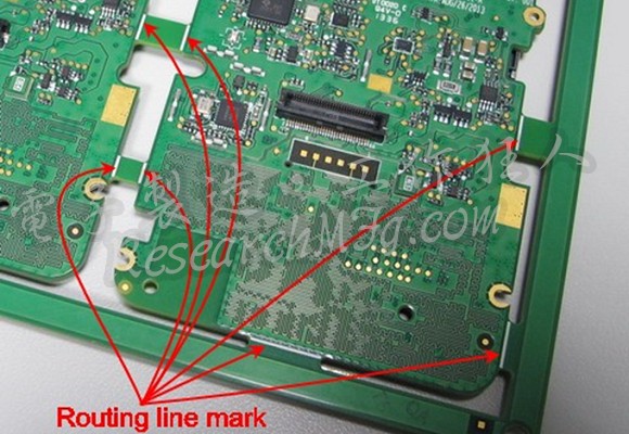
We all know that when producing PCBs and PCBAs, multiple individual PCBs are usually combined into one larger panel, a process called panelization, to improve production efficiency. Typically, these individual boards are arranged in a neat and consistent manner with the same orientation. However, when the PCB has an irregular shape or special requirements, a mirrored panel or flipped panel design might be used. While this design can improve efficiency in the SMT production line and reduce material costs, it may also come with certain design and production challenges. In this article, we will explore these issues and consider potential solutions.

read more…》

Oct24
Causes and Prevention of PCB Warping and Bending After Reflow

Causes and Prevention of PCB Warping and Bending After Reflow

A reader recently asked: “In surface mount assembly, PCBs often warp or bend after going through the reflow process, which can cause issues like open solder joints or tombstoning. How can we overcome this?”

To be honest, the reasons behind PCB warping or bending may vary, but they can generally be traced back to the stress applied to the PCB exceeding what the material can handle. When stress is uneven across the PCB or when different areas of the PCB resist stress unevenly, warping or bending occurs.

read more…》

Oct17
Benefits and Drawbacks of Using Nitrogen (N2) in SMT Reflow Ovens: Optimizing Soldering Quality and Reducing Oxidation

Benefits and Drawbacks of Using Nitrogen (N2) in SMT Reflow Ovens: Optimizing Soldering Quality and Reducing Oxidation

The primary purpose of adding Nitrogen (N2) to the SMT reflow oven is to reduce oxidation on the soldering surface and improve the wettability of the solder joints. Nitrogen is a colorless, odorless, and chemically inactive gas. It belongs to the category of inert gases, meaning it doesn’t easily react with most metals to form compounds. By using nitrogen to replace the oxygen in the environment, we can prevent metals from reacting with oxygen, thus avoiding oxidation.

(This is a summary article, and the views expressed may not be entirely accurate. If you find any issues, feel free to share your opinions or feedback.)

read more…》

Oct03
What Causes Wave-Like Wrinkles or Cracks in Solder Joints After Reflow?

What Causes Wave-Like Wrinkles or Cracks in Solder Joints After Reflow?

These soldering wrinkles appeared quite a while ago, but Workingbear recently came across a similar situation on an online forum. Thinking others might encounter the same issue, I decided to document it for both personal reference and to share with everyone.

Workingbear had previously noticed that some data transmission cable samples from a supplier had solder joints on the internal PCBA with wave-like wrinkles and what looked like cracks. At first, it was assumed that these were caused by cracked flux residue. However, even after cleaning the flux with alcohol, the same wave-like wrinkles were still visible, indicating that the issue was actually with the solder itself.

read more…》

Sep26
The Role of Immersion Gold and Electroplated Gold in PCB Soldering

The Role of Immersion Gold and Electroplated Gold in PCB Soldering

Workingbear previously wrote an article about how insufficient gold thickness in the ENIG surface treatment of a PCB led to the oxidation of Electroless Nickel, weakening solder joints and causing components detachment during plug and unplug. However, many sources explain that gold’s primary role in PCB surface finishes is to prevent nickel oxidation by acting as a barrier. Gold (Au) doesn’t strengthen  solder joints and may form brittle intermetallic compounds (IMCs) like AuSn and AuSn2, leading to gold embrittlement.

Recommended reading: Two Major Potential Problems with ENIG PCB Pads (Black Nickel and Phosphorus-rich Layers) and Preventive Measures

read more…》