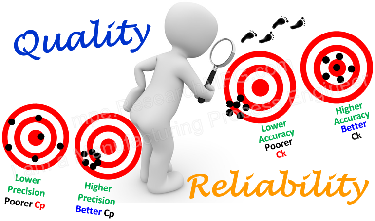
Do you know the difference between quality and reliability? These two terms often get confused, but if you dig deeper, they actually mean different things. So how do you tell them apart?
(The following is just Workingbear’s personal opinion and doesn’t claim to be 100% accurate.)
Quality is a broad concept. What exactly is “high quality”? People often say that Japanese products are high-quality and well-loved. So in a general sense, quality refers to how well a product meets or exceeds people’s expectations or satisfaction compared to other similar products.


