Working for manufacturer engineering couple years. Sharing the manufacturing experience, skill, DFx, design, and information. Be care of this blog is personal share and content may not be 100% correctly.
Figure: Using the Red Dye Penetration Test to Check BGA Solder Joints for Open Solder or Head-in-Pillow (HIP) Defects
At first glance, analyzing returned electronic products or BGA failures doesn’t seem all that complicated. In reality, however, many new engineers have no idea where to begin when a failed unit is returned from a customer or the field. Even worse, I’ve watched new engineers accidentally destroy critical evidence before they even start the investigation. Once the evidence is gone, so are many of the clues needed to find the real root cause.
Troubleshooting a failed electronic product is surprisingly similar to solving a crime in CSI or NCIS. Instead of rushing to conclusions, you start by gathering evidence and carefully examining every clue. From there, you develop possible root-cause hypotheses and test them one by one until the real culprit reveals itself. Ideally, you should also be able to reproduce the failure. If you can’t recreate it, there’s always a chance you’ve only found a symptom rather than the actual root cause.
To be honest, troubleshooting engineering problems follows the same principles as an 8D Report or any structured problem-solving methodology. The key is to work through the investigation step by step instead of jumping to conclusions. It may seem tedious at times, but a systematic approach helps prevent important details from being overlooked. In fact, those tiny details often provide the breakthrough you’re looking for. As the saying goes, the devil is in the details.
Successful troubleshooting comes down to one thing: attention to detail. Finding the root cause is rarely about making brilliant guesses—it’s about carefully collecting evidence, analyzing the facts, and eliminating possibilities one by one. This requires a very different mindset from developing new products, where creativity and innovation often take center stage. In reality, however, much of the day-to-day work in product development focuses on refining existing designs, improving manufacturability, and reducing production costs.
When analyzing a failed product, always start with the least invasive methods and work your way toward more destructive techniques. The general sequence should be:
In other words, inspect the entire product first. If you cannot identify the problem, move on to non-destructive testing. Only after those methods fail should you perform localized destructive testing, and reserve complete destructive analysis as the final option.
The following is Workingbear’s personal troubleshooting workflow, developed from years of hands-on experience. It’s based largely on memory and practical field work, so there may certainly be techniques I’ve overlooked. If you have additional suggestions or better approaches, I’d love to hear them.
1. If the Returned Product Is Still Fully Assembled, Start with a Visual Inspection and Functional Test
Figcaption: Defect analysis Step 1. If the Returned Product Is Still Fully Assembled, Start with a Visual Inspection and Functional Test
Before taking anything apart, verify that the product actually exhibits the failure reported by the customer.
Always compare the customer’s failure description with the symptoms you observe. You’d be surprised how often the wrong unit gets shipped back for analysis. Just as frequently, the frontline personnel misdescribe the problem altogether. Before investing hours in troubleshooting, make sure you’re investigating the correct product.
Sometimes the returned unit isn’t defective at all. It may simply be a false reject, also known as No Defect Found (NDF). The actual problem may lie with the customer’s power supply, operating environment, or another external factor rather than the product itself.
Some failures don’t appear immediately after power-up. Others occur only intermittently. In these situations, it’s often helpful to let the product run continuously for at least 24 hours using an automated test program while performing normal operating functions. The goal is to reproduce the customer’s reported issue.
Whenever possible, ask the customer about the conditions under which the failure occurred before—or as soon as—you receive the returned product. Understanding the operating environment, usage pattern, and timing of the failure can significantly narrow down the possible root causes.
Also, don’t forget to inspect the enclosure for signs of impact damage. A product that has been dropped may suffer internal damage that isn’t immediately obvious from the outside.
2. If the Product Has Already Been Disassembled or Only the PCB Is Returned, Begin with a Thorough PCB Visual Inspection
Some returned boards fail because of contamination rather than manufacturing defects.
I’ve personally found dead cockroaches and even spider webs inside electronic equipment. Warm, humid electronics make surprisingly attractive homes for insects. Liquid contamination is another common cause of failures—coffee and soft drinks are probably the most frequent offenders.
In other cases, an electrical short may have already burned components or damaged PCB traces. Burn marks, corrosion, contamination, and other physical evidence can often be identified during a careful visual inspection.
Use a microscope whenever possible, and inspect the entire board—not just the area where you expect the failure to be. Treat it like a crime scene. Examine every trace, solder joint, and component carefully. Don’t overlook even the smallest clue.
3. After the Visual Inspection, Perform Functional Testing Again—and Check CPU Temperature
If the customer returns only the PCBA, perform a functional test after completing the visual inspection. The reason is the same as described in Step 1: confirm that the reported failure can actually be reproduced.
Even when the entire system is returned, it can still be useful to functionally test each individual PCBA. Many electronic products contain multiple circuit boards, and testing them separately helps isolate which board is actually responsible for the failure.
For PCBAs that only fail after operating for some time, monitor the temperature of key devices—especially the CPU or processor—using either a thermometer or a thermal imaging camera.
If a major IC heats up abnormally, it often indicates an electrical problem. Conversely, if the CPU never warms up at all, that may suggest it isn’t operating or booting properly. Temperature measurements can provide valuable diagnostic clues long before more invasive analysis becomes necessary.
4. Measure Circuit Signals to Pinpoint the Faulty Component
If a visual inspection and basic functional testing still don’t reveal the cause of the failure, it’s time to dig deeper with electrical measurements.
This is when you’ll typically see hardware engineers armed with a digital multimeter (DMM) and an oscilloscope, probing test points throughout the circuit. They’re checking for open or short circuits, incorrect voltage levels, missing signals, or timing issues between ICs. The goal is to narrow down which component—and even which pin or signal—is responsible for the failure.
This happens to be one of Workingbear’s weaker areas. My background is in mechanical engineering rather than circuit design, so I’ll leave the detailed signal analysis to the electronics experts.
Once electrical measurements indicate that the BGA (Ball Grind Array) package is the likely source of the problem, the next step is to determine whether the failure is caused by a short circuit or an open circuit. Ideally, the electrical engineer should also identify the suspected solder ball or signal involved before any physical failure analysis begins.
5.1 If the BGA Has a Short Circuit
In most cases, an X-ray inspection is the fastest way to identify the BGA shorts problem.
However, BGA shorts are relatively uncommon in products returned from customers, since the assembly should have already passed electrical testing before leaving the factory.
Keep in mind that some short circuits cannot be detected by X-ray alone. In these cases, consider whether the problem could be caused by flux residue combined with moisture, creating a leakage path between adjacent solder joints. These “micro-shorts” are most commonly observed during environmental testing, particularly under high-temperature, high-humidity conditions. Although it’s relatively rare for customer returns to be caused by flux residue, it shouldn’t be ruled out—especially with fine-pitch BGAs.
Another possible cause is CAF (Conductive Anodic Filament) formation inside the PCB. CAF is an EM (electrochemical migration) phenomenon that can create conductive paths between closely spaced conductors, especially between vias, plated through holes (PTHs), and nearby PCB traces when a bias voltage is present.
5.2 If the BGA Has an Open Circuit
An open-circuit failure can have several possible causes.
5.2.1 Broken Bond Wire or Bond Lift Inside the IC Package
Sometimes the failure occurs inside the semiconductor package itself. A broken bond wire or a lifted bond wedge can usually be identified using X-ray inspection.
5.2.2 Open BGA Solder Joint
The first priority is to narrow down which solder ball is suspected of failing. Once the suspected location is identified, inspect it using X-ray.
HIP (Head-in-Pillow) or HoP (Head on Pillow) defect
Unfortunately, conventional 2D X-ray systems often cannot clearly detect common BGA solder joint defects such as Head-in-Pillow (HIP) or partial open solder joints. Whenever possible, use a 3D X-ray CT system, which provides much better visibility of individual solder joints. A 2.5D X-ray system with an oblique viewing angle can also be an effective alternative.
If the suspected solder joint is located near the outer edge of the BGA, optical inspection may also be worthwhile. Using a microscope or a flexible fiber-optic scope, you can often inspect the outer one or two rows of solder balls—as long as nearby components don’t block the view.
Interestingly, Head-in-Pillow (HIP) defects are most commonly found around the outer rows of BGA solder balls. This is largely because both the PCB and the BGA substrate can warp during the reflow soldering process, causing incomplete contact between the solder ball and the PCB pad.
Unfortunately, even after careful optical inspection, you’ll often come away disappointed because the defect simply isn’t visible from the outside.
5.2.3 If Everything Else Fails, Use a Red Dye Penetration Test or Cross-Section Analysis
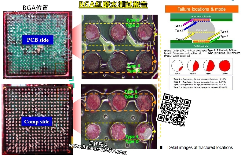
Figure: Using the Red Dye Penetration Test to Detect Cracked BGA Solder Joints
Before discussing these methods, it’s important to emphasize that both are destructive failure analysis techniques. Once performed, the sample cannot be restored. For this reason, they should always be reserved as the final step in the investigation and should ideally be performed by experienced failure analysis specialists.
If you only have one failed board available, Workingbear generally recommends going directly to cross-section analysis.
Cross-sectioning provides much higher resolution and allows you to examine not only the BGA solder joints but also the internal PCB structure. Remember that an open circuit isn’t always caused by a defective solder joint—it may also originate from an internal PCB interconnection, such as a plated via or an internal copper layer.
Since cross-section analysis requires physically cutting through the PCBA, you should identify the exact BGA device—and preferably the suspected solder ball—before sending the sample to the lab. This saves both time and money because preparing a high-quality cross section is extremely labor-intensive.
If time and budget permit, or if the faulty solder ball cannot be identified beforehand, the laboratory may section the BGA row by row until the defect is found. While this approach is expensive and time-consuming—failure analysis labs typically charge by the hour—it significantly increases the likelihood of locating the actual failure.
Patience is essential. You may need to inspect dozens or even hundreds of solder joints under a microscope. Fatigue can easily lead to missed defects, so it’s often a good idea to have two engineers independently verify the findings.
If you have multiple boards exhibiting the same failure, then a Red Dye Penetration Test becomes a practical option.
Compared with cross-sectioning, the red dye test is a relatively simple and less expensive destructive analysis method. It is primarily used to identify cracked solder joints, Head-in-Pillow (HIP) defects, and similar mechanical failures. Interpreting the dye patterns correctly requires experience, but for widespread solder joint failures, it can be extremely effective because it allows all of the BGA solder joints to be evaluated at the same time.


 To be honest, troubleshooting engineering problems follows the same principles as an 8D Report or any structured problem-solving methodology. The key is to work through the investigation step by step instead of jumping to conclusions. It may seem tedious at times, but a systematic approach helps prevent important details from being overlooked. In fact, those tiny details often provide the breakthrough you’re looking for. As the saying goes, the devil is in the details.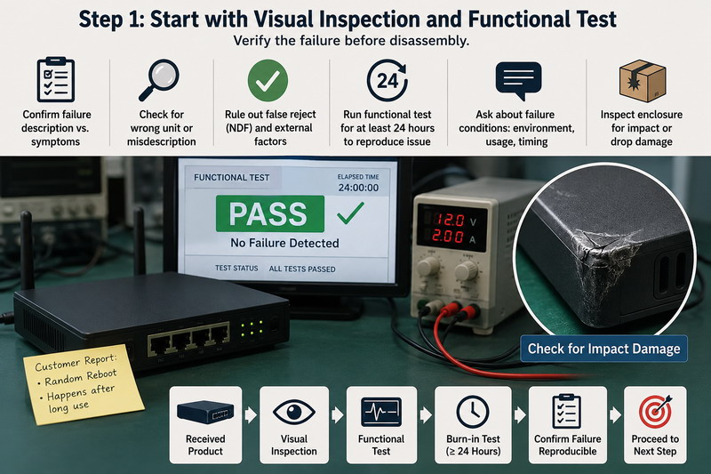




![[Case Study] Troubleshooting a Customer Complaint – Keypad Malfunction Caused by Oil & Powder Contamination on the PCB](https://mpe.researchmfg.com/wp-content/uploads/2025/Oil_on_PCB_summary-mpe-170x85.jpg "[Case Study] Troubleshooting a Customer Complaint – Keypad Malfunction Caused by Oil & Powder Contamination on the PCB")


Leave a Reply