

When producing large volumes of PCBs (Printed Circuit Boards), multiple individual boards are often combined into one large panel. This panelized form is then processed through automated SMT production lines to improve efficiency and reduce costly machine idle time.
When deciding how to connect the boards in a panel, you must also consider how they will be separated later. Otherwise, you might end up with a panel that’s easy to assemble, but difficult to de-panel.
Some people may think panelization is just putting boards together side-by-side and deciding how many to combine. Maybe rearrange oddly shaped boards to optimize material usage — nothing worth discussing, right? Not quite. There are several important considerations:
Some PCBs have strict outline and dimensional requirements because the shape or size might be used later for fixture positioning. If two boards are placed directly against each other, even slight deviation during de-paneling can result in one board being slightly oversized and the other undersized.
No matter what de-paneling method you use, removing material is unavoidable. Without buffer points between boards, de-paneling tolerance becomes harder to control. That’s why PCB factories typically use precise routing machines to pre-cut most of the outline, leaving only ribs or other small connections in non-critical areas. The location and number of these connection points also affect the strength of the entire panel.
The mainstream connection methods used for PCB (Printed Circuit Board) panelization today include the following:
1. V-Cut (V-Groove): A V-shaped groove is cut symmetrically on both the top and bottom sides of the PCB. This groove is used to separate and connect adjacent individual boards or break-away rails. In later stages, the boards can be separated manually by snapping or by using scoring equipment.
Terminology: What is V-cut? Why PCB need to design V-cut on it?
2. Tabs / Ribs: Between two adjacent individual boards or break-away rails, a routed slot about 3–5 mm wide at least is designed. Structural support areas are connected using tabs or ribs. During production, a router depaneling machine is required to cut and separate the boards.
Recommended reading: What Is Router Cutting for PCB Depaneling? Advantages and Disadvantages Explained
3. Stamp Holes (also called mouse bites, break-away holes, or perforation holes): This concept is similar to tabs/ribs connection. A routed slot about 3–5 mm wide (sometimes wider depending on tab width) at least is added between two individual adjacent boards or rails. Structural areas are supported by tabs or ribs, but small perforated holes are added where the tabs meet the boards. These holes make it easier to break the boards apart using simple hand tools during the depaneling process. Of course, it also can be separated by router depaneling machine.
Recommended reading: PCB Edge Removal and De-paneling: Stamp Hole Design
After completing the PCBA assembly, the mainstream methods used for depaneling include the following:
- V-Cut Scoring Machine:
This equipment is used to separate PCBs along pre-cut V-grooves. - Router Depaneling Machine:
A rotating bit is used to cut along routed slots, separating individual boards with high accuracy. - Manual Depaneling:
Boards can be separated manually by snapping them apart or using semi-automatic tools or fixtures. However, this method is generally not recommended, as it can easily cause stress-related damage to components or solder joints. - Laser Depaneling Machine:
A laser beam is used to cut the board material, offering high precision and minimal mechanical stress. - Punch Depaneling Machine:
This method uses a punch-and-die set to separate boards. It is rarely used nowadays. Some PCB manufacturers may still use it, so this article will not discuss this method in detail.
Because PCB material is primarily resin and copper foil, it has thickness and is both hard and tough — making them difficult to break by hand unless… you’re a bodybuilder.
V-cut Panel Connection and De-paneling
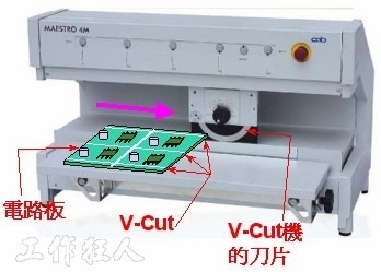 The proper way to separate V-cut panels is with a V-cut scoring machine, which is typically used only for boards specifically designed with V-cuts. Of course, you can redundantly de-panel them using a router, laser cutting machine, or even manually too.
Recommended reading: What is V-cut? Why PCB need to design V-cut on it?
Generally, the remaining thickness of a V-cut area is about one-third of the original board thickness. This reduces the risk of boards accidentally snapping during production and handling, while still allowing easy separation when needed.
Originally, V-cut panels were designed for manual de-paneling back when wave-soldered through-hole components dominated assembly. These joints were strong and could handle bending stress. But once SMT (Surface Mount Technology) became common, manual bending was no longer recommended — it can easily cause cracked solder joints or damaged components.
Recommended reading: PCB De-Paneling: V-cut scoring de-paneling and removing board edges
Advantages of V-cut:
-
Simple and fast de-paneling
-
No special fixtures required
Disadvantages of V-cut:
-
De-panel edges often form protruding “> <” shapes with burrs and debris
-
Only straight-line connections are possible — no jumps or arcs
-
Components must be kept away from V-cut lines to avoid tool interference
-
PCB thickness under 1.0 mm is not recommended due to weak strength
Tabs/Ribs Panel Connection and Router De-paneling
 Tabs/Ribs connections are typically separated using a depanel router, or sometimes laser cutting. They cannot be separated with V-cut scoring or manual bending.
A router is essentially a CNC cutting machine. It uses high-speed rotating bits along programmed paths to cut ribs. Because of the spinning tool, custom fixtures are required to hold PCBs in place. Dust collection is also needed to prevent debris from sticking to boards or being inhaled by workers.
Advantages of router de-paneling:
-
Minimal bending stress on the PCB
-
Reduces risk of solder cracks and component damage
-
Works well for boards unsuitable for V-cut
-
Clean cut edges with better dimensional accuracy
Disadvantages:
-
Higher processing cost compared to V-cut
Laser cutting can also be used for rib connections. It produces:
-
No dust
-
No burrs
-
No mechanical stress
-
Programmable cutting paths
However, lasers cannot cut through copper, because resin and copper require different laser energy settings. This can usually be avoided through PCB design. Router bits also shouldn’t cut into copper areas because it quickly wears the tool.
Stamp Holes (Mouse Bite) Panel Connection and De-paneling
You can think of the “stamp hole” panel design as adding a row of small holes—called mouse bites—at both ends of each tab that connects the individual boards. The idea is to make it easier to break the boards apart later using simple hand tools like diagonal cutters. Because of that, stamp holes are more commonly used for prototypes, small production runs, or low-cost manual assembly operations.
However, from a quality control perspective, Workingbear strongly recommends treating stamp-hole panels the same way as tab-routed ones—meaning they should still be separated using a router or a laser cutting machine, rather than by hand.
Advantages of stamp holes:
- They allow panel separation without expensive equipment.
Disadvantages of stamp holes:
- When boards are snapped apart with pliers or cutters, the break line usually leaves rough burrs that must be sanded or filed off. Poor stamp-hole design can also cause excessive burrs that stick out from the board edge, which may cut fingers or create assembly issues.
- Stamp holes can be thought of as small perforations at the ends of tabs/ribs. Their purpose is to allow easy manual separation using diagonal cutters or similar tools. They are commonly used for samples, small production quantities, or low-cost home-based assembly factories.
Related Posts:
- What Are PCB Cross-out Boards (X-out Boards)?
- Do PCB Designs Require Reserving Board Edges and Grooves for Routers De-Paneling Machines?
- Why is Panelization and Break-away Tab Necessary in PCB Manufacturing, then De-paneling after PCBA is Completed?


?")


Leave a Reply