Working for manufacturer engineering couple years. Sharing the manufacturing experience, skill, DFx, design, and information. Be care of this blog is personal share and content may not be 100% correctly.
With the rapid adoption of smartphones, the trend toward miniaturized electronic products, and the EU’s requirements for lead-free manufacturing, Electroless Nickel Immersion Gold (ENIG) surface treatment PCB has become a popular choice for many electronic products. This is largely due to its simplicity and lower cost compared to other surface treatments, as well as its numerous advantages, including:
Excellent reworkability: ENIG allows for multiple soldering processes without compromising quality.
Superior flatness: Perfect for fine-pitch components.
Strong resistance to oxidation: Suitable for long-term storage.
Versatility: Can be used for contact circuits like keypads.
For these reasons, an increasing number of electronics manufacturers have chosen ENIG as the surface finish for their PCBs.
However, in daily SMT soldering processes, we often encounter two major potential issues with ENIG-treated PCBs: Nickel Corrosion and Phosphorus-Rich Layers. These two issues are considered critical drawbacks of the ENIG process. They are not only difficult to detect during production due to their hidden nature, but they also often result in batch-level solder joint reliability problems. Once these issues occur, they are challenging—sometimes even impossible—to repair, leading to severe consequences.
When using ENIG-treated PCBs for SMT assembly, one of the most common concerns is the so-called “black pad” issue, also known as black nickel. However, many people don’t fully understand what “black nickel” or “black pads” actually are. In this article, Workingbear will attempt to explain these terms and share some insights about the “black nickel” or “black pad” problem in ENIG-treated PCBs.
(Note: Workingbear does not claim to have a 100% accurate understanding of ENIG-related black pad issues. The following content may contain inaccuracies, and your corrections or feedback are welcome.)
The formation of “black nickel” in ENIG is primarily attributed to two factors: Phosphorus-Rich Layers and Nickel Oxidation.
Phosphorus-Rich Layers
The “phosphorus” in ENIG comes from the electroless nickel plating layer. During the subsequent gold immersion process, phosphorus does not react and remains between the gold and nickel layers, creating a phosphorus-rich (P-rich) layer. This can lead to embrittlement of the solder joint, reducing its strength.
Nickel Oxidation
Nickel oxidation typically involves complex nickel oxide compounds (NixOy, where x and y are numbers). This occurs during the gold immersion process when the nickel surface undergoes excessive oxidation (the metal nickel atoms oxidize into nickel ions, which is a form of oxidation). Additionally, the large atomic size of gold atoms (atomic radius of 144 pm) leads to irregular deposition, forming a rough, porous grain structure. As a result, the gold layer fails to completely cover the underlying nickel layer, leaving parts of the nickel exposed to air. Over time, the exposed nickel continues to oxidize, eventually forming nickel rust under the gold layer. This oxidation process interferes with soldering and creates significant challenges.
Why Nickel Oxidation Impacts Soldering Quality
Most solder alloys, such as SAC305, SAC307, SnBi, and SnBiAg, use tin (Sn) as their primary base. When a PCB passes through the reflow oven, the tin reacts with the nickel in ENIG to form an intermetallic compound (IMC) called Ni3Sn4. If the nickel layer is already oxidized, it becomes difficult to form an ideal IMC. Even if IMC does form, it may be inconsistent and unevenly distributed at the interface between the solder and the nickel. This weakens solder joint strength.
To illustrate, imagine building a brick wall where cement holds the bricks together. The cement represents the IMC. If some areas of the wall lack cement, the wall becomes structurally weak—this is similar to how a poorly formed IMC affects solder joints.
A More Effective Solution: ENEPIG
An alternative surface treatment for PCBs is Electroless Nickel Electroless Palladium Immersion Gold (ENEPIG). This method effectively mitigates the “black nickel/black pad” issue. However, due to its higher cost, ENEPIG is currently only adopted for high-end PCBs, CSPs, or BGA applications. For those seeking greater soldering reliability, ENEPIG is an excellent solution despite the higher price.
The following content is adapted from Luo Daojun’s work at ‘China Saibao Laboratory,’ with some wording adjustments.
Two Major Potential Issues with ENIG Pads and Their Prevention
The Basics of the ENIG Process
One of the greatest advantages of ENIG (Electroless Nickel Immersion Gold) surface treatment on PCBs is its simplicity in manufacturing. Essentially, the process only requires two main chemical solutions—electroless nickel plating and acidic gold solution—along with a few auxiliary chemicals. The typical ENIG process begins with depositing a layer of nickel onto the copper pad through chemical plating. The thickness of the nickel layer is controlled by adjusting the time and temperature of the reaction. Afterward, the freshly deposited nickel’s active surface allows the pad to be immersed in the acidic gold solution, where a chemical displacement reaction takes place. During this process, gold from the solution is deposited onto the pad surface, while some of the nickel dissolves into the gold solution. The deposited gold layer gradually covers the nickel layer, and once the nickel is fully covered, the reaction automatically stops. After cleaning off contaminants from the pad surface, the ENIG process is complete. At this point, the gold layer is typically about 0.05 µm (2 µ”) thick or even thinner, making ENIG a process that is relatively easy to control and cost-effective compared to electrolytic nickel-gold plating.
However, this thin layer of gold primarily serves as an oxidation barrier for the nickel layer. If the gold layer fails to provide adequate protection, the nickel layer can become exposed to air, leading to oxidation and corrosion, or it may be over-etched by the gold solution. These issues result in the so-called “black nickel” or “black pad” phenomenon. What’s particularly challenging is that the surface of the pad may still appear shiny and golden to the naked eye, making it difficult to visually detect any issues. For this reason, it is crucial to strengthen the quality inspection of ENIG-treated PCBs before assembly.
The quality of the nickel layer primarily depends on the formulation of the nickel plating solution and the temperature control during chemical deposition. It is also influenced by the process of treating the layer with acidic gold solution. The chemical nickel plating process forms the layer through an autocatalytic reaction between hypophosphite and nickel salt on the pad surface. This layer contains a certain amount of phosphorus (P). Studies show that the optimal phosphorus content in the nickel layer should range between 7% and 10%. If the plating solution is not properly maintained or the temperature is poorly controlled, the phosphorus content may deviate from this range.
When the phosphorus content is too low, the nickel layer becomes highly prone to corrosion, especially from acidic gold solution etching. On the other hand, when the phosphorus content is too high, the nickel layer’s hardness increases significantly, leading to poor solderability and negatively impacting the formation of reliable solder joints.
If the nickel layer has a low phosphorus content and the chemical displacement reaction during gold plating is not well-controlled, the resulting gold layer may contain numerous cracks. Acidic gold solution residues left during the cleaning process will accelerate corrosion of the exposed nickel layer, ultimately leading to the formation of black nickel, also known as black pads.
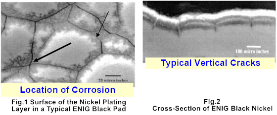
A typical black pad is shown in Figure 1, and a cross-section of a black pad is shown in Figure 2. From the cross-sectional image, distinct vertical cracks—a hallmark of black nickel—are clearly visible.
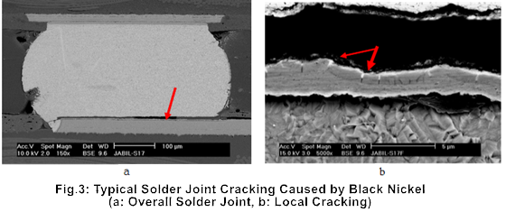
Once black nickel forms, the gold layer on the ENIG surface may still appear shiny, giving the illusion of an intact and well-processed pad. However, during high-temperature soldering, the protective gold layer will rapidly dissolve into the solder paste, leaving the corroded and oxidized nickel exposed. This nickel cannot effectively form intermetallic compound (IMC) with the molten solder, resulting in a significant decrease in solder joint reliability. Solder joints affected by black nickel are prone to cracking under minimal external forces. A typical example of solder joint cracking caused by black nickel is shown in Figure 3.
Formation and Risks of Phosphorus-Rich Layers
In the ENIG surface treatment process, it is the nickel layer, not the gold layer, that forms an IMC alloy with the solder paste during soldering. The typical intermetallic compound (IMC) formed is Ni3Sn4. However, phosphorus in the nickel layer does not participate in this chemical reaction. Phosphorus is evenly distributed throughout the nickel layer, but as the nickel reacts to form the alloy, excess phosphorus accumulates in certain areas, forming a phosphorus-rich layer concentrated at the edges of the alloy layer.
If the phosphorus-rich layer becomes too thick, it significantly weakens the overall strength of the solder joint. When external stress is applied to the solder joint, failure is most likely to occur at the weakest link—the phosphorus-rich layer. This directly impacts the reliability of the solder joint.
This issue is particularly critical in high-temperature lead-free soldering processes, where poor process control often leads to thicker intermetallic compounds. This results in more excess phosphorus, making the phosphorus-rich layer more pronounced and the solder joint’s reliability increasingly vulnerable.
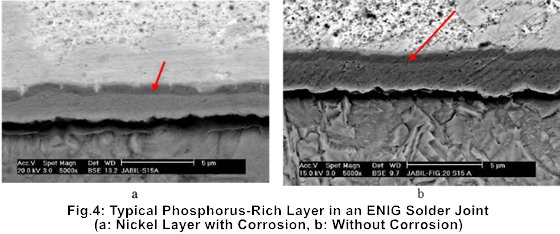
A typical phosphorus-rich layer can be seen in Figure 4 as the dark band between the intermetallic compound and the nickel layer. Energy dispersive spectroscopy (EDS) analysis confirms that this dark region contains an extremely high concentration of phosphorus. Numerous failure case studies have demonstrated that the presence of a phosphorus-rich layer is one of the primary causes of solder joint cracking and failure.
Prevention and Control of Black Nickel and Phosphorus-Rich Layers
Although the formation of black nickel and the appearance of phosphorus-rich layers can be difficult to detect and prevent due to their hidden nature, understanding the root causes allows us to find effective methods for prevention and control.
Preventing Black Nickel
During the manufacturing process, it’s crucial to maintain the plating solution and control the process temperature to ensure the nickel-phosphorus ratio in the plating layer remains optimal. The acidic gold solution should also be carefully maintained; if its corrosiveness becomes too strong, adjustments should be made promptly.
For end-users, there are three primary methods to detect and prevent black nickel:
Scanning Electron Microscope (SEM):
Use SEM to perform microscopic surface inspections of the pad’s plating, checking for cracks in the gold layer. Additionally, use Energy Dispersive Spectroscopy (EDS) to analyze whether the phosphorus content in the nickel layer is within the normal range.
Manual Soldering and Strength Testing:
Perform manual soldering on sample pads and measure the pull or push strength of the solder joints. If the strength is abnormally low, black nickel might be present.
Acidic Gas Corrosion Test:
Expose ENIG samples to acidic gas corrosion tests. If you observe surface discoloration or powder formation, it suggests cracks in the gold plating and indicates the possible presence of black nickel.
Among these methods, the second one—manual soldering and strength testing—is the simplest and quickest to implement. These testing methods allow you to detect potential issues in ENIG boards early, before assembly begins. By identifying problems early, you can avoid producing large quantities of circuit board assemblies with reliability issues, keeping losses to a minimum.
Preventing Phosphorus-Rich Layers
To prevent the formation of phosphorus-rich layers, it’s essential to maintain the correct nickel-to-phosphorus ratio in the nickel plating layer. Beyond that, focus on controlling the soldering process—specifically the soldering time and temperature. The thickness of the intermetallic compound (IMC) layer should be kept within an optimal range of 1–2 microns (µm) is better. Excessively thick IMC layers not only lead to reliability problems but also result in an overly thick phosphorus-rich layer, further compromising solder joint strength and durability.

 and How to Prevent Them")


 Plating on Components or Circuit Boards in the Electronics Industry")


Leave a Reply