
Workingbear’s company was having a tough time with a strange issue: intermittent micro-short circuits inside the layers of the PCB. Since the shorts didn’t show up near any components, it was really hard to figure out what was wrong.
Recently, we made a breakthrough. We finally got a faulty PCB that consistently showed the issue. After working with the PCB manufacturer to analyze it, we found the likely cause: CAF (Conductive Anodic Filament)—a type of metallic filament caused by electrochemical migration (ECM), which is known to cause failures in PCBs.
At last, we had a clear direction to investigage. Before that, our customer was getting very frustrated because we couldn’t find the root cause.
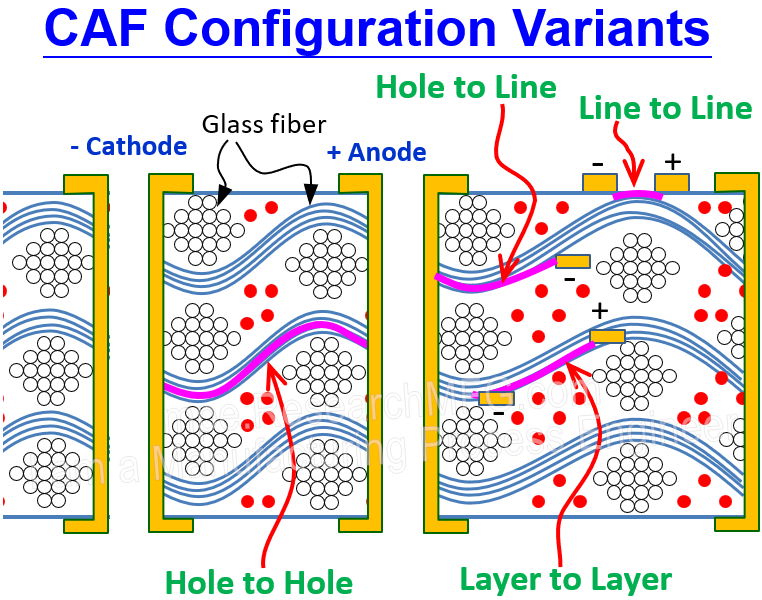
Finding an actual CAF symptom like this isn’t easy. First, you need to locate the short on the PCB. Then, cut nearby traces step by step to narrow it down. It best to figure out which via-to-via or trace-to-trace, or which copper layer is causing the short. Once the area is small enough, you must do a cross-section cut to try tp catch the micro-short. But even then, you’re not guaranteed to see the short.
- If you’re not familiar with PCB structure or glass fibers, check out the article “Introduction to the structure, characteristics and precautions of Printed Circuit Board materials”
- And if you don’t know what CAF is, read “What is CAF (Conductive Anodic Filament) in PCBs? and How to Prevent It”
Doing a cross-section isn’t simple. If it’s done poorly or by someone without experience, they might miss the problem entirely—or worse, the grinding process might create false signs that lead to the wrong conclusion.
The first time we tried, we sent samples to two 3rd party labs. Lab A said everything looked fine. Lab B said they saw gaps in the glass fibers that might lead to CAF. But since those samples didn’t always show the short problem, it was hard to say which lab was right.
Later, we finally got a PCB that definitely had the short circuit symptom. Our engineer took it straight to the PCB factory and had them cut it open on the spot. This time, they clearly saw signs of CAF.
After that, the factory started blaming our PCB design. They said our vias and blind vias were too close together. At first, they said 0.4 mm spacing was okay, but now they were saying it needed to be at least 0.5 mm. The design we sent had only 0.1 mm between holes edge to edge, and now they wanted to change it to 0.5 mm—what a headache!
But our engineer stood firm. He told PCB suppliers they had reviewed the design before fabric the PCB and didn’t raise any spacing issues. Also, since the factory builds PCBs every day, they should know more about CAF than we do. Even if our design had some risks, the factory should still take most of the responsibility for this case. We didn’t ask them for money, but we did ask them to give us a plan to fix the issue and prevent it from happening again.
Here are the improvements suggested by the PCB factory to reduce CAF issues (experienced folks, feel free to chime in):
-
Change in PP (Prepreg) filler material: The filler was changed from S1000 to S1000H. The factory said S1000H has better resistance to CAF.
-
Change in PP stacking and ratio: Change the core’s prepreg from a stack of five layers of 7628 to four layers of 7628 with a higher resin content (RC). Since the core became thinner, they added one more layer of 3313 prepreg above and below the core to maintain the original PCB thickness.
PP Resin Formulation Filler Z-CTE Drilling/
Desmear/
PTH performanceAnti-CAF ability T260 Min. T280 Min. Td °C288°C/10s
Number of solder dipsS1000 Brominated Epoxy Resin Composite filler, total content around 20%3.4% Comparable performance NA 60 10 335 15 S1000H Brominated Epoxy Resin Composite filler, total content around 30%2.8% Comparable performance Greater advantage 60 20 348 20 -
Drilling feed rate adjustment: The drilling speed was reduced from 80 to 50.
Since Workingbear was directly involved in this failure analysis, I learned a lot through this experience and discussions. It gave me a deeper understanding of PCB structures and materials, and I also picked up some valuable skills in finding CAF issues.
When you suspect CAF on a PCB, you cafn start by using electrical testing and cutting nearby traces to narrow down the short. Before doing a cross-section, you can use ultrasonic scanning to check if the board has delamination. Be sure to remove the components first so the ultrasound won’t be affected. Then you can decide whether to grind the board horizontally or vertically based on the scan. There’s also a newer solution using 3D X-Ray CT, which might help detect this kind of defect without damaging the board.
CAF happens when there’s a voltage difference (bias) and moisture between two nearby nodes (like traces, vias, or layers). Under these conditions, copper ions (Cu2+) start to migrate along gaps in the glass fiber bundle, from the anode (high voltage side) to the cathode (low voltage side). This is called electrochemical migration (ECM).
The short usually starts off weak and intermittent. Copper at the anode oxidizes into Cu+ or Cu++ and travels down a bad path along the glass fibers. Along the way, it meets electrons coming from the cathode. The ions turn back into copper metal, then oxidize again, and so on—gradually building a copper path toward the cathode. That’s why it’s also called copper migration.
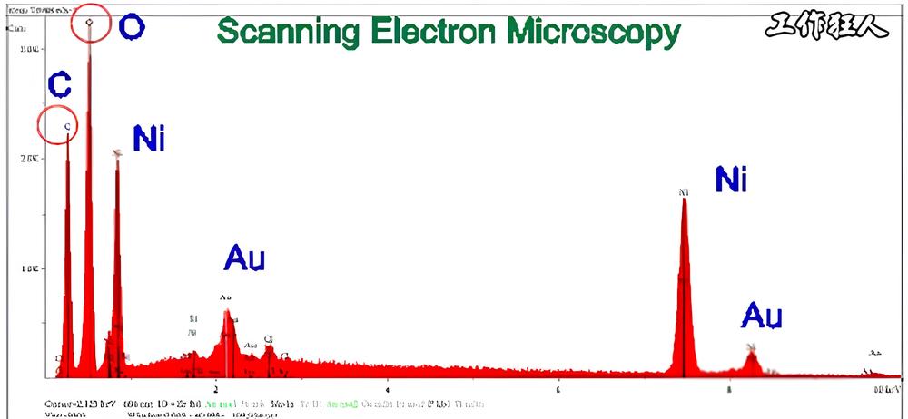
But in our case, the EDX test didn’t detect copper—it showed gold (Au) instead. That likely means there was a problem during the ENIG (Electroless Nickel Immersion Gold) surface finishing process.
▼ The image below is from a lab cross-section. You can see cracks in the glass fabric, and some conductive material starting to grow along the fiber gaps—but it hasn’t shorted yet.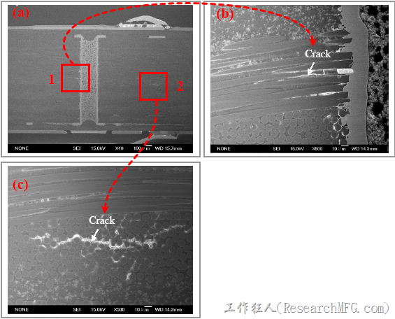
▼ When you suspect CAF, start by testing the PCB electrically and cutting traces to isolate the short circuit. You might need to remove components to avoid interference.
▼ Keep narrowing down the location, and use the Gerber file to check if any vias or traces are too close together.
▼ Here’s a cross-section of a PCB where the short circuit was still present. Even before applying any chemical treatment, you can already see a thin copper “wicking” bridging between a via and a blind via. However, this might just be copper smearing caused by the grinding process.
▼ After chemical treatment, this image shows a cleaned section. EDX detected gold (Au) between the via and blind via. (Later, the factory said the gold was from a coating they applied!)
▼ First EDX result showing gold between the via and blind via.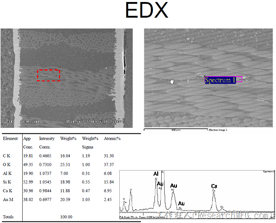
▼ Second EDX result showing gold in a similar position.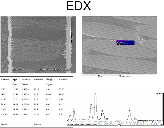
- Problem Analysis and Solving: 8D report
- What is the Popcorn Effect in PCBs and Electronic Components?
- What is CTE (Coefficient of Thermal Expansion)? What is α2-CTE? How Does CTE Affect PCB Quality?
- What is IMC (Intermetallic Compound)? How does IMC relate to PCB solder joint strength? Are there IPC standards for IMC thickness?



![[Case Study] Troubleshooting a Customer Complaint – Keypad Malfunction Caused by Oil & Powder Contamination on the PCB [Case Study] Troubleshooting a Customer Complaint – Keypad Malfunction Caused by Oil & Powder Contamination on the PCB](https://mpe.researchmfg.com/wp-content/uploads/2025/Oil_on_PCB_summary-mpe.jpg)


I am look for an expert to issue an opinion letter for a PCB failure due to CAF. Let me know if you are anyone you know could help with such a matter. It is not for a legal case but to confirm our own finding but with an expert opinion behind it.
Frank Shum
Filamento
Frank,
I’m not a CAF expert—my knowledge is limited to a general understanding of CAF.
You may send your case to my email, but I can’t guarantee a response or a definitive opinion.