Oct24
Causes and Prevention of PCB Warping and Bending After Reflow

Causes and Prevention of PCB Warping and Bending After Reflow

A reader recently asked: “In surface mount assembly, PCBs often warp or bend after going through the reflow process, which can cause issues like open solder joints or tombstoning. How can we overcome this?”

To be honest, the reasons behind PCB warping or bending may vary, but they can generally be traced back to the stress applied to the PCB exceeding what the material can handle. When stress is uneven across the PCB or when different areas of the PCB resist stress unevenly, warping or bending occurs.

read more…》

Oct17
Benefits and Drawbacks of Using Nitrogen (N2) in SMT Reflow Ovens: Optimizing Soldering Quality and Reducing Oxidation

Benefits and Drawbacks of Using Nitrogen (N2) in SMT Reflow Ovens: Optimizing Soldering Quality and Reducing Oxidation

The primary purpose of adding Nitrogen (N2) to the SMT reflow oven is to reduce oxidation on the soldering surface and improve the wettability of the solder joints. Nitrogen is a colorless, odorless, and chemically inactive gas. It belongs to the category of inert gases, meaning it doesn’t easily react with most metals to form compounds. By using nitrogen to replace the oxygen in the environment, we can prevent metals from reacting with oxygen, thus avoiding oxidation.

(This is a summary article, and the views expressed may not be entirely accurate. If you find any issues, feel free to share your opinions or feedback.)

read more…》

Oct03
What Causes Wave-Like Wrinkles or Cracks in Solder Joints After Reflow?

What Causes Wave-Like Wrinkles or Cracks in Solder Joints After Reflow?

These soldering wrinkles appeared quite a while ago, but Workingbear recently came across a similar situation on an online forum. Thinking others might encounter the same issue, I decided to document it for both personal reference and to share with everyone.

Workingbear had previously noticed that some data transmission cable samples from a supplier had solder joints on the internal PCBA with wave-like wrinkles and what looked like cracks. At first, it was assumed that these were caused by cracked flux residue. However, even after cleaning the flux with alcohol, the same wave-like wrinkles were still visible, indicating that the issue was actually with the solder itself.

read more…》

Sep26
The Role of Immersion Gold and Electroplated Gold in PCB Soldering

The Role of Immersion Gold and Electroplated Gold in PCB Soldering

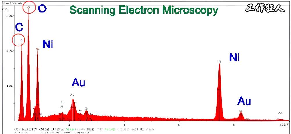
Workingbear previously wrote an article about how insufficient gold thickness in the ENIG surface treatment of a PCB led to the oxidation of Electroless Nickel, weakening solder joints and causing components detachment during plug and unplug. However, many sources explain that gold’s primary role in PCB surface finishes is to prevent nickel oxidation by acting as a barrier. Gold (Au) doesn’t strengthen  solder joints and may form brittle intermetallic compounds (IMCs) like AuSn and AuSn2, leading to gold embrittlement.

Recommended reading: Two Major Potential Problems with ENIG PCB Pads (Black Nickel and Phosphorus-rich Layers) and Preventive Measures

read more…》

Sep19
Does the Gold Thickness in ENIG PCBs Affect Component Detachment?

Does the Gold Thickness in ENIG PCBs Affect Component Detachment?

The solder pads at the site where the component fell off show signs of black pad discoloration, and most of the pads were pulled off with the component and are still attached to the component leads. It is speculated that the detachment occurred at the Electroless Nickel (EN) layer or the phosphorus-rich (P-rich) layer."

Do you know how the thickness of the gold layer in ENIG surface-finished PCBs impacts soldering quality? What role does the gold layer play in PCBA soldering? How could the detachment of electronic components from a PCB be related to the gold thickness in ENIG? Should the gold layer be as thick as possible?

For a while, the SMT contractor managed by Workingbear got into a dispute with the PCB manufacturer. Both parties were debating the gold thickness specifications for ENIG (Electroless Nickel Immersion Gold) surface-finished PCBs. The issue arose because the EMS (Electronic Manufacturing Services) factory recently used a batch of ENIG PCBs, and during the final assembly after surface mount and board-level testing, components were found detaching from the PCB. Initially, the SMT factory strongly believed that the detachment was caused by the “black pad” issue commonly associated with ENIG. From the appearance, the pads where the components had detached showed the characteristic black pad color. Most of the pads had come off the board entirely, sticking to the component leads. The theory was that the solder fracture might have occurred at the Electroless Nickel (EN) layer or the phosphorus-rich (P-rich) layer.

read more…》