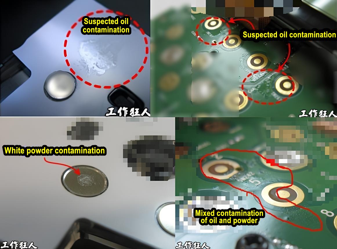
When we discover unknown contaminants on printed circuit boards assembly (PCBA) or electronic products, how do we determine what they are and where they come from? Do we rely on experience, or do we use scientific instruments for analysis? What methods are commonly used in the industry to detect and analyze contaminants?
If you’re a fan of the “I’m a Manufacturing Process Engineer“ blog, you may have noticed that Workingbear often mentions two main methods for contamination analysis:
- EDX/EDS (Energy-Dispersive X-ray Spectroscopy)
- FTIR (Fourier-Transform Infrared Spectroscopy)
Both of these techniques use spectral analysis, comparing the sample’s spectrum with known elements or compounds to identify what’s present. While the principles behind them differ, their comparison methods are quite similar.
If you’re willing to spend the money—or rather, if your budget allows—there are commercial laboratories that offer these testing services. If you’ve watched the TV show NCIS, you’ve probably seen the character Abby performing chemical analysis on contaminants and using a computer to match the results. If you’re interested, you might want to check it out!
However, it’s important to note that EDX/EDS and FTIR operate using different energy sources, meaning they each have their own strengths and limitations. Neither method can identify every possible substance, and their coverage is not universal.
In fact, besides EDX/EDS and FTIR, there are many other methods for contamination analysis, each with its own strengths and limitations. Some examples include:
- AES (Auger Electron Spectroscopy)
- AFM (Atomic Force Microscopy)
- TOF-SIMS (Time-of-Flight Secondary Ion Mass Spectrometry)
- XPS (X-ray Photoelectron Spectroscopy)
If you’re unsure which method to use, it’s best to consult a commercial lab to get more information and choose the most suitable technique for your specific needs.
Since Workingbear primarily uses EDX/EDS and FTIR in daily work, the following sections will focus on these two methods and what has been learned from experience.
(Note: Workingbear is not an expert in this field, so the following explanations may have inaccuracies. If any experts happen to read this, feel free to provide corrections or guidance!)
EDX/EDS (Energy-Dispersive X-ray Spectroscopy)

Depending on the size of the equipment, EDX/EDS testing often requires cutting the sample to fit inside the machine. This means that in most cases, the sample must be destroyed or modified to fit within the device.
The reason why EDX/EDS is widely used in the industry today is not because it’s the best method, but because it comes with Scanning Electron Microscopy (SEM). SEM provides high-resolution, deep-depth grayscale images of the sample’s surface and near-surface, similar to taking a black-and-white photograph.
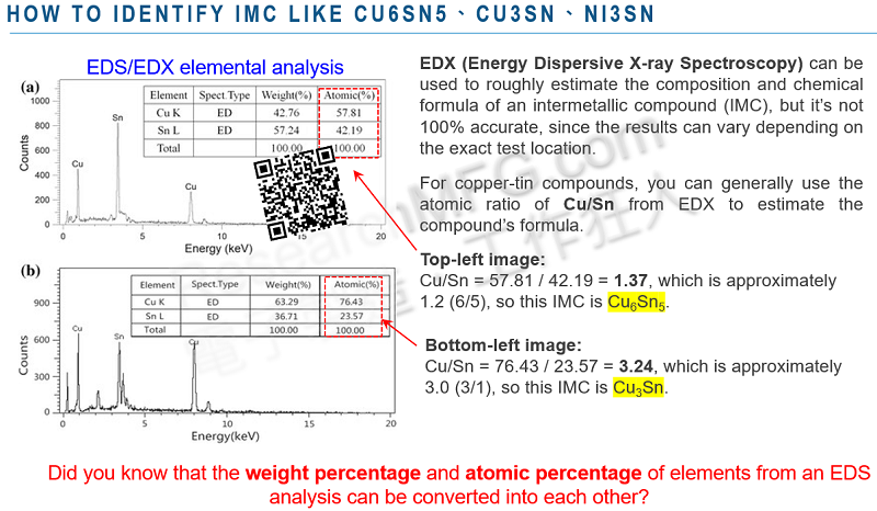
EDX/EDS can only detect the elemental composition of a sample—it cannot determine its chemical formula. For simple compounds, it may be possible to estimate the chemical formula based on molecular weight. For example, when analyzing the intermetallic compound (IMC) formed after soldering on a copper-based PCB, EDX can help determine whether it is Cu₅Sn₆ or Cu₃Sn, but this is largely based on inference rather than direct measurement.

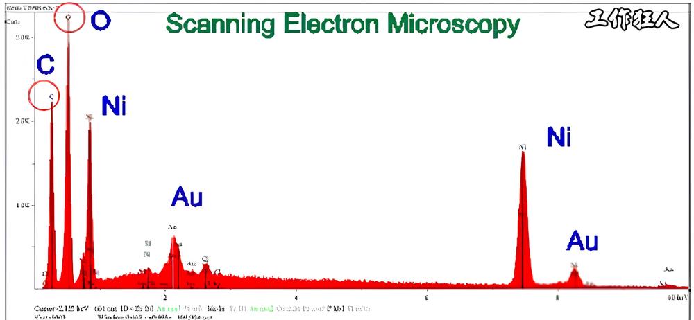
In general, EDX is best suited for elemental analysis of a material’s surface. In the electronics industry, it is commonly used to inspect PCB surface treatments, such as checking for defects in ENIG plating or measuring the phosphorus (P) content in cross-sectioned samples to ensure it is within acceptable limits.
However, EDX cannot be used to analyze flux or solvents. This is because flux and solvents are composed of chemical compounds, which means their structures are defined by molecular formulas rather than just elemental composition. Additionally, EDX cannot detect hydrogen (H), helium (He), or lithium (Li) due to their low atomic numbers. Some manufacturers now claim that their latest EDX systems can detect lithium, but this is still under debate.
FTIR (Fourier-transform infrared spectroscopy)

FTIR works based on the principle of infrared optical interference. When an infrared light source passes through a beam splitter, it is divided into two beams—one directed toward a fixed mirror and the other toward a moving mirror. After reflecting off these mirrors, the beams recombine into a single infrared light beam. Due to the path difference caused by the moving mirror, the final recombined light undergoes constructive and destructive interference, producing infrared light with varying energy levels. (This concept is actually covered in middle or high school textbooks!)
When this infrared beam interacts with a sample—whether by transmission, reflection, or attenuated total reflection (ATR)—it creates an interference pattern detected by the system. By applying a Fourier Transform (FT), this pattern is converted into an infrared absorption spectrum, which we can analyze.
Since different compounds absorb infrared energy at different wavelengths, they produce unique spectral patterns. This allows us to identify different compounds based on their spectra. However, in reality, the number of chemical compounds is far greater than we can imagine, and most materials are mixtures of multiple compounds. Identifying a substance using a database match is difficult unless the compound is already documented in the system. That’s why FTIR analysis typically requires a reference sample. To improve accuracy, the suspected substance should be tested alongside a known reference compound, allowing for direct spectrum comparison to determine if they match.
For example, when analyzing flux residues, different brands may have similar formulations but slightly different compound ratios, leading to distinct FTIR spectra. The best approach is to send in a suspected chemical for FTIR comparison, increasing the chances of identifying the unknown substance.
For more insights, check out this case study:
[Investigating PCB Button Contamination: The Unexpected Culprit?]
Related Posts:


Leave a Reply