


HASL stands for Hot Air Solder Leveling and is one of the most common PCB surface finishes. It is commonly referred to simply as HASL or a solder coating. During the HASL process, the finished PCB is immersed in molten solder so that the exposed copper surfaces are coated with solder. Hot-air knives then remove excess solder and level the coating to provide a solderable surface.
The solder coating protects the exposed copper from oxidation and provides a solderable surface for component assembly. HASL equipment can generally be divided into two types: vertical and horizontal systems, each with its own advantages and disadvantages. HASL is available in both leaded and lead-free versions, but this article focuses primarily on lead-free HASL.
Advantages of HASL-Finished PCBs:
-
One of the main advantages of HASL is its low cost. It is generally less expensive than ENIG (Electroless Nickel Immersion Gold), although it is usually slightly more expensive than OSP (Organic Solderability Preservative).
-
HASL generally has a longer storage life than OSP. Its storage life is basically comparable to ENIG. If moisture is properly controlled and the HASL and ENIG finish thicknesses and processes meet the required specifications, solderability normally remains acceptable during storage for up to about one year. One thing to watch for, however, is the risk of PCB delamination when a PCB that has been stored for a long period is exposed to the high temperatures of reflow. This can affect long-term reliability. If a HASL PCB has been stored for more than one year, additional attention should be paid to the condition of the finish because intermetallic compound (IMC) growth caused by copper-tin diffusion can become a concern.
-
HASL can readily bond with the solder in solder paste or molten solder, providing good wetting and soldering performance. This is because the HASL coating itself is primarily composed of solder. However, this good solderability is generally more applicable to the first reflow. The same advantage may not necessarily remain for the second reflow surface, which we will discuss in more detail in the disadvantages section.
Disadvantages of HASL-Finished PCBs:
-
If the HASL coating is primarily pure tin, it can be susceptible to tin whisker formation, which may eventually cause electrical shorts and make it less suitable for fine-pitch components. Tin whiskers are driven by differences in the stresses generated by thermal, chemical, and mechanical factors. These factors can produce compressive stress in the tin layer, which is then released through whisker growth. Many studies have shown that pre-plating the copper surface with a layer of nickel as a barrier layer, followed by the tin coating, can help suppress tin whisker growth.
-
In a double-sided reflow process, the surface solder on the second-reflow side has already been exposed to the high temperature of the first reflow. As a result, the solder coating can partially remelt during the second reflow and form solder beads or droplet-like protrusions under the influence of gravity. This can make the second side of the PCB uneven and affect the accuracy of solder paste printing, which in turn can affect solder joint quality.
-
If there is too much time between the first and second reflow processes, the solder coating on the second-reflow side can remain exposed to air and become oxidized, forming a passivation layer. This oxidation can negatively affect solderability during the second reflow.
-
If the HASL coating on a double-sided PCB is too thin, the solder layer on the second-reflow side can be consumed during the first reflow as additional tin-copper IMC forms. In other words, the first reflow can consume part of the solder coating on the second-reflow side. As a result, there may not be enough remaining solder coating during the second reflow to properly bond with the solder in the solder paste. This can lead to non-wetting and reduced solder joint strength. As a general guideline, the HASL coating thickness should be at least 2.54 µm for large copper areas, with a minimum of 2 µm. For QFPs and surrounding components, 5 µm or more is recommended. For BGA pads, 11.4 µm or more is recommended.
-
Like OSP, HASL uses a copper-based substrate. Therefore, shortly after soldering, the joint initially forms Cu6Sn5 IMC, which generally provides good mechanical strength. However, after prolonged use, Cu6Sn5 can gradually transform into Cu3Sn, which can be detrimental to solder joint reliability and may eventually contribute to component detachment. Adding nickel (Ni) to the HASL coating or solder paste formulation can help slow the formation of Cu3Sn and improve the long-term reliability of HASL-finished PCBs.
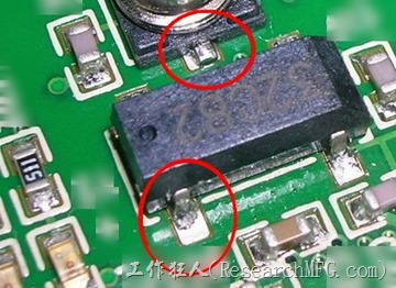
The image above shows poor solder wetting on a HASL-finished PCB. It is not an image from this particular case.
Workingbear’s Recommendations When Selecting HASL-Finished PCBs
- When selecting HASL, consider the overall combination of single- or double-sided assembly, component pitch, and process control requirements.
- Personally, I recommend using HASL primarily for single-sided assembly whenever possible. This helps avoid many of the problems associated with the second reflow side.
- A tin-whisker mitigation strategy should be included in the HASL PCB process.
- When using HASL-finished PCBs for SMT assembly, I recommend using a nickel-containing (Ni) solder paste formulation to slow the growth of Cu3Sn and improve long-term solder joint reliability.
- If HASL must be used on a double-sided PCB, consider placing fine-pitch components and components that are particularly sensitive to solder paste volume on the first-reflow side during PCB layout. This can help reduce the risk of insufficient soldering and short circuits.
- HASL coating thickness should be strictly controlled. I recommend making it one of the key inspection items during IQC (Incoming Quality Control).
- For SMA (Surface Mount Assembly), the recommended interval between the first and second reflow processes for a HASL-finished PCB is 24 to 72 hours. If the interval will exceed this range, the PCB should be vacuum-packaged again or stored in a nitrogen cabinet to minimize exposure to air and prevent excessive formation of oxidized or passivated tin on the surface, which could negatively affect subsequent solderability.
Related Posts:
- 霧錫(Matte tin)與亮錫 (Bright tin)的差別
- 何謂「銅」基地與「鎳」基地電路板(PCB)?
- Causes of Poor Solderability on HASL Finished PCBs (Data Collection and Analysis)
- The Purpose of Nickel (Ni) Plating on Components or Circuit Boards in the Electronics Industry
- What is the Purpose of Surface Finishes for PCB? A Summary of the Pros and Cons of Common PCB Finishes



Leave a Reply